Definition : When conductor (metal or semiconductor) carrying a current is placed in a transverse magnetic field, an electric field is produced inside the conductor in a direction normal to both the current and the magnetic field. This phenomenon is known as “Hall effect” and the generated voltage is called “Hall voltage”.
This effect is named after the physicist E.H.Hall, who discovered this effect in 1879.
Importance of hall effect
The importance of hall effect is :
- To determine the charge carrier concentration.
- To determine the sign of charge carriers.
- To determine the mobility of charge carriers if conductivity of the material is known.
Hall effect in N-type semiconductors
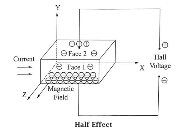
Let us consider an n-type material to which the current is allowed to pass along x-direction from left to right (electrons move from right to left) and the magnetic field is applied in z-directions, as a result Hall voltage is produced in y direction as shown in Fig.

Since the direction of current is from left to right the electrons move from right to left in x-direction as shown in Fig.
![]()
Now due to the magnetic field applied the electrons move towards downward direction with the velocity ‘v‘ and cause the negative charge to accumlualte at face (1) of the material as shown Fig. Therefore a potential difference is established between face (2) and face (1) of the specimen which gives rise to field EH in the negative y direction.
Eqn – 1
Here, the force due to potential difference = -eEH
Eqn – 2
Force due to magnetic field = -Bev
At equilibrium eqn. (1) = eqn. (2)
-eEH = -Bev
Eqn – 3
EH = Bv
We know the current density Jx in the x direction is
Jx = -ne ev
Eqn – 4
![]()
Substituting eqn. (4) in eqn. (3) we get
![]()
Eqn – 5
EH = RH . Jx . B
where ‘RH‘ is known as the Hall coefficient, given by
![]()
The negative sign indicates that the field is developed in the negative y direction.
Hall effect in P-type semiconductors
Let us consider a p-type material for which the current is passed along x-direction from left to right and magnetic field is applied along z-direction as shown in Fig. Since the direction of current is from left to right, the holes will also move in the same direction.
![]()
Now due to the magnetic field applied, the holes move towards the downward direction with velocity ‘v’ and accumulates at the face (1) ad shown in Fig.
A potential difference is established between face (1) and (2) in the positive y-direction.
Eqn – 7
Force due to the potential difference = eEH
Eqn – 8
Force due to magnetic field = Bev
Since hole is considered to be an electron with same mass but positive charge negative sign is not included.
At equilibrium eqn. (7) = eqn. (8)
eEH = Bev
Eqn – 9
EH = Bv
We know current density Jx = nh ev
Eqn- 10
![]()
where nh is hold density
Substituting eqn. (10) in (9) we get

Equation (11) represents the Hall coefficient and the positive sign indicates that the Hall field is developed in the positive y direction.
Hall coefficient in terms of Hall volatge
Half Coefficient (RH) is defined as the Hall field developed per unit current density per unit applied magnetic field.
If the thickness of the sample is ‘t’ and the voltage developed is ‘VH‘ then Hall voltage
Eqn – 12
VH = EH . t
Substituting eqn. (11) in eqn.(12), we have
Eqn – 13
VH = RH Jx B . t
If ‘b’ is the width of the sample then area of the sample = b.t
Eqn – 14
Current density = ![]()
∴ Half coefficient ![]()
Experimental determination of Hall Effect
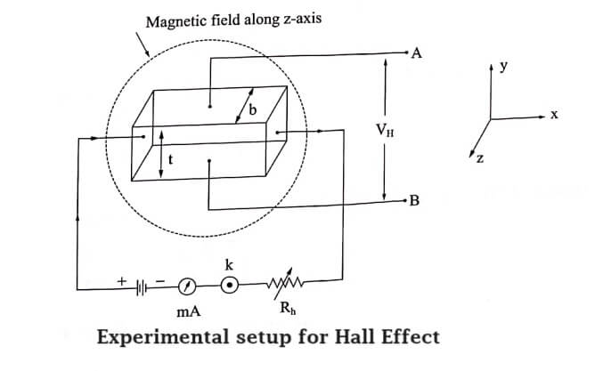
A semiconductor slab of thickness ‘t’ and breadth ‘b’ is taken and current is passed using the battery as shown in Fig.
The slab this placed between the pole pieces of an electromagnet so that current direction coincides with x-axis and magnetic field coincides with z-axis. The Hall voltage (VH) is measured by placing two probes at the center of the top and bottom faces of the slab (y-axis).
If B is magnetic field applied and the VH is the Hall voltage produced, then the Hall coefficient can be calculated from the formula
Eqn – 1
![]()

Mobility of charge Carriers
In general the Hall co-efficient can be written as
Eqn – 2
![]()
The above expression is valid only for conductors where the velocity is taken as the drift velocity.
But for semiconductors velocity is taken as average velocity so RH for an ‘ n’ type semiconductor is modified as

We know the conductivity for n type is = σe = n e μe
Eqn -4
![]()
Eqn. (3) can be rewritten as
Eqn – 5
![]()
Substituting eqn. (5) in (4) we get,
Eqn – 6
![]()
The mobility of electron is in an n-type semiconductor is
Eqn – 7
![]()
Similarly for p-type Semiconductor, the mobility of hole is
Eqn – 8
![]()
Thus by finding Hall voltage, Hall coefficient can be calculated and thus the mobility of the charge carriers (μe and μh) can also be determined.
Application of Hall Effect
Determination of semiconductor type: For an n-type semiconductor the Hall coefficient is negative whereas for a p-type semiconductor it is positive. Thus, the sign of the Hall coefficient can be used to determine whether a given semiconductor is n-type or p-type.
Calculation of carrier concentration : By knowing the value of RH, the Hall coefficient, the carrier concentration is to be determined.
![]()
Determination of mobility: If the conduction is due to one type of carriers and by measuring the conductivity and the Hall coefficient of a sample, the mobility of the charge carrier can be calculated.
Determination of flux density: Using a semiconductor sample of known hall coefficient, the magnetic flux density can be determined.
Measurement of power flow : It is used to find the power flow in an electromagnetic wave.
Hall effect sensors : Hall effect sensors are used in various applications such as automotive speedometers, fluid flow sensors, current sensors and pressure sensors.
Industrial applications : Hall effect joysticks are used to control hydraulic valves.
| Read More Topics |
| Variation of carrier concentration with temperature |
| Elemental and compound semiconductors |
| Success of classical free electron theory |


