1. What is a semiconductor?
The materials in which the electrical conductivity lies between conductors and insulators are called semiconductors. They have resistivity value between 10-4 to . The electrical conductivity of semiconductor increases when we add impurities and by increasing the temperature and it is contrary to the metals. They have negative temperature Coefficient of resistance and which are formed by covalent bonds.
2. Distinguish between Elemental semiconductors and Compound semiconductors.
| S . No | Elemental semiconductors | Compound semiconductors |
| 1. | These are made from single element. | These are made from compound (mixed) element. |
| 2. | These are made from IV group elements. | These are made from III and V [or] II and VI group of elements. |
| 3. | These are called as indirect band gap semiconductor (electron – hole recombination takes place through traps ). | These are called as direct band gap semiconductor (electron – hole recombination takes place through directly ). |
| 4. | Heat is produced in the recombination. | Photons are produced in the recombination. |
| 5. | Life time of charge carriers is more due to indirect recombination. | Life time of charge carriers is less due to direct recombination. |
| 6. | Current amplification is more. | Current amplification is less. |
| 7. | These are used for making diodes, transistor ,etc.
Examples : Ge , Si |
These are used for making LED, laser diodes ,etc.
Examples : GaA, GaP, CdS, MgO |
3. What are intrinsic semiconductors?
A semiconductor in which holes and electrons are created only by thermal excitation across the energy gap is called an intrinsic semiconductor. A pure crystal of silicon or germanium is an intrinsic semiconductor.
In an intrinsic semiconductor the number of holes in valence band is equal to number of electrons in the conduction band. The Fermi level for an intrinsic semiconductor lies midway in the forbidden gap.
4. Define mobility of the semiconductor.
Mobility of is defined as the ratio of drift velocity to the applied electric field.

5. Define Diffusion current.
Diffusion current is defined as the motion of charge carriers from the region of higher concentration to the region of lower concentration.
6. What are extrinsic semiconductors?
It is an impure semiconductor made by doping process thereby reducing the band gap up to 0.01eV . There are two types of extrinsic semiconductors.
1.N-type and 2. P-type.
7. Differentiate N-type and P-type semiconductor.
| S. No | N-type | P-type |
| 1. | It is donor type. | It is acceptor type. |
| 2. | Impurity atom is pentavalent. | Impurity atom is trivalent. |
| 3. | There is donor level. | There is acceptor level. |
| 4. | Donor level lies close to the bottom of the conduction band. | Acceptor level lies close to the top of the valence band. |
8. Sketch the variation of fermi level in intrinisic semiconductor.
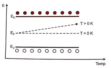
- At , T = 0K the fermi level lies exactly in midway between conduction band and valence band.
- At T > 0K, the fermi level rises slightly upward since mh* > me* .
9. What is the effect of impurity states in a semiconductor?
The carrier concentrations are increased causing high electrical conductivity, band gap energy is reduced up to 0.01eV and additional energy levels are produced.
10. What are donor and acceptor impurities?
A semiconductor in which the impurity atoms are added by doping process is called Extrinsic semiconductor. The addition of impurities increases the carrier concentration and conductivity. There are two types of impurities :
- Donor impurity which leads to N-type semiconductor.
- Acceptor impurity which leads to P-type semiconductor.
Donor impurity means it donate the electrons to the semiconductor materials and Acceptor impurity means it ready to accept an electron to form the covalent bond in semiconductor materials.
11. State law of mass action.
It states that in an Extrinsic semiconductor, the product of electron concentration and hole concentration, produced by the doping process, is a constant.
ie., NP = ni2 = a constant.
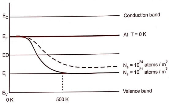
12. Sketch the variation of fermi level with temperature for various concentration in P- type semiconductor.

- When T = 0K , EF = (EA + En) i.e., at T = 0K , the fermi level lies at mid way between the acceptor level and valence level.
- When temperature increases, some of the electrons from valence band will go to acceptor energy level [EA ] . Therefore the fermi level shifts upward. At high temperature 500K , the fermi level reaches intrinsic level Ei .
- If the impurity atoms are increased from 1021 atoms/m3 to 1024 atoms/m3 , the hole concentration increases and hence the fermi level decreases.
13. Sketch the variation of Fermi level with temperature for various concentration in N-type semiconductor.
- When
![T=0 K, E_F=\left[\frac{E_A+E_V}{2}\right]](https://pedagogyzone.com/wp-content/ql-cache/quicklatex.com-ae37443b51686f9d170ae8da139dc606_l3.png "Rendered by QuickLaTeX.com") , i.e., at T = 0 K , the fermi level lies at mid way between the donor level and conduction level.
, i.e., at T = 0 K , the fermi level lies at mid way between the donor level and conduction level. - When temperature increases, some of the electrons from donor level [ED] may be shifted to conduction band and vacant sites will be created in donor level [ED]. Therefore the fermi level shifts downward and at high temperature 500K, the fermi level reaches intrinsic level Ei .
- If the impurity donor atoms are increased from 1021 atoms/m3 to 1024 atoms/m3 , the electron concentration increases and hence the fermi level increases.
14. What is pair production or generation?
When an energy is supplied to the semiconductor, the covalent bonds are broken and the electrons are raised from valence band to conduction band and a vacant site is created in the valence band. It is called pair production or generation of electron-hole pair.
15. What is Recombination?
An electron jumps from the conduction band to the valence band vacant site is called as band to band recombination of electron – hole pair. During band to band recombination the excess energy is released in the form of light photon. The recombination also occurs via recombination centre and traps.
16. Define Hall effect ?
If a semiconductor or a conductor carrying current (I) is placed in a magnetic field (B), an electric field is produced in the direction normal to both the current and magnetic field. The generated voltage (VH) is called the Hall voltage and the field is called Hall field (EH ).
17. What are the applications of hall effect ?
- The sign of charge carriers can be determined.
- The carrier concentration can be determined using

- The mobility of charge carriers in measured directly

- Electrical conductivity can be determined.[ σ = nqμ ]
- It can be used to determine whether the given material is metal, insulator, or semiconductor and the type of the semiconductor.
- From the measured Hall voltage, the unknown magnetic field can be measured provided the value of Hall coefficient for the slab in known.
18. Define N-type and P-type semiconductor.
If pentavalent (Phosphorous, arsenic, antimony) impurities are doped, then the free electrons are produced, this semiconductor is called N-type semiconductor. If trivalent [Aluminium, Gallium, indium] impurities are doped, then the holes are produced, then this semiconductor is called N-type semiconductor
19. Define diffusion current.
In addition to drift current, there is also another current called diffusion current. Diffusion current does not takes place in metals.
Diffusion current is defined as the motion of charge carriers from the region of higher concentration to the region of lower concentration.