Bit addresses for I/O – Microcontroller 8051
Microcontroller 8051 contains four I/O ports. They are Port 0, Port 1, Port 2 and Port 3. All ports are 8 bit ports. So totally it contains 32 I/O pins that connects the 8051 to the outside world. Port 0 pins may be served as inputs, outputs or when used together, as a bidirectional low order address and data bus for external memory. Port 1 pins have no dual functions.
Therefore, its output latch is connected to the external pin through only the output driver. Port 2 may be used as an input/output port similar in operation to port 0. The alternate use of port 2 is to supply high order address byte in conjuction with the port 0 low order byte to address external memory. Port 3 is an input/output port similar to port 1. Port 3 pins are, also used for alternate functions.
When the port pin may be used as an input, a 1 must be written to its corresponding port latch by the program, the pin to float in a high impedance state, and which makes the pin is essentially connected to the input buffer.
When port is used as an output, the pin latches that transferred to its output pin. The 578 are programmed are alternate functions of Port 3 are shown in the table below.
I/O Bit addresses for RAM
- The 128 byte internal RAM of microcontroller 8051 is organized into three distinct areas. Thirty two bytes from 00H to 1FH that make up 32 working registers organized as four banks of 8 rigister each. The four register banks are numbered 0 to 3 and are made up to 8 registers named R0 to R7.
- Bit and Byte addressable area of 16 bytes occupies RAM byte addresses 20H to 2FH, forming a total of 128 addressable bits. They are addressed as 00H to 7FH.
- Only Byte addressable area of 80 bytes occupies RAM byte addresses from 30H to 7FH. The 128 bytes of RAM can be accessed in byte size by using various addressing modes such as direct addressing and register indirect addressing. The bit nstructions addresses of internal RAM can be accessed only by using direct addressing. The bit and byte addresses of internal RAM with bit addressable locations are shown in the image.
I/O Programming – Microcontroller 8051
In microcontroller 8051, the I/O devices should be treated as memory. So memory mapped I/O scheme is only possible for accessing I/O devices. In the 64 Kbyte external datal memory map, some spaces are reserved for 1/0 devices. Hence MOVX instructions are used for accessing both external memory and I/O devices. These instructions are only accumulator specific instructions, because the data are only moved from or to accumulator (A register).
Example 1 : Write an ALP for receiving an 8 bit data placed in memory location 2400 H, and place it in Ro register.
MOV DPTR,#2400H
MOVX A,@DPTR
MOV R0,A
HALT SJMP HALT
The first instruction load DPTR with an address 2400H. The second instruction, moves the data placed in memory location 2400H to A register. The third instruction places that data in R0 register. During the execution of this instruction, the data is moved through port 0.
Example 2 : Write an ALP for storing the data placed in register RO to memory location 2500H.
MOV A,RO
MOV DPTR,#2500H
MOVX @DPTR,A
HALT SJMP HALT
The first instruction moves the data inregister R0 to Accumulator. The second instraction loads DPTR with an address 2500H. The third instruction stores the data in the memory location 2500H. During the execution of this instruction the data is actually moved from microcontroller 8051 to memory through port 0.
I/O Bit manupulation Programming
By using the bit manipulation instruction instructions, we can perform various functions like clear, set, complement, AND logic, OR logic, move and control jump in bit level. The single bit data may be placed rither in the internal bit and byte addressable RAM or in the bit and byte addressable SFR.
The first instruction moves the data placed in memory location 2FH to the carry flage. The second instruction moves the data placed in carry flag to port pin P2.0.
Read modify write feature
Some instructions read a port, read the latch and others read the pin. The instructions that read the latch rather than the pin are the ones that read the value, possibly change it and then rewrite it to the latch. These are called read modify write instructions. When the destination operand is a port or a port bit, these instructions read the latch rather than the pin. The instructions shown in the following table are read modify write instructions.
Timer/Counters – Microcontroller 8051
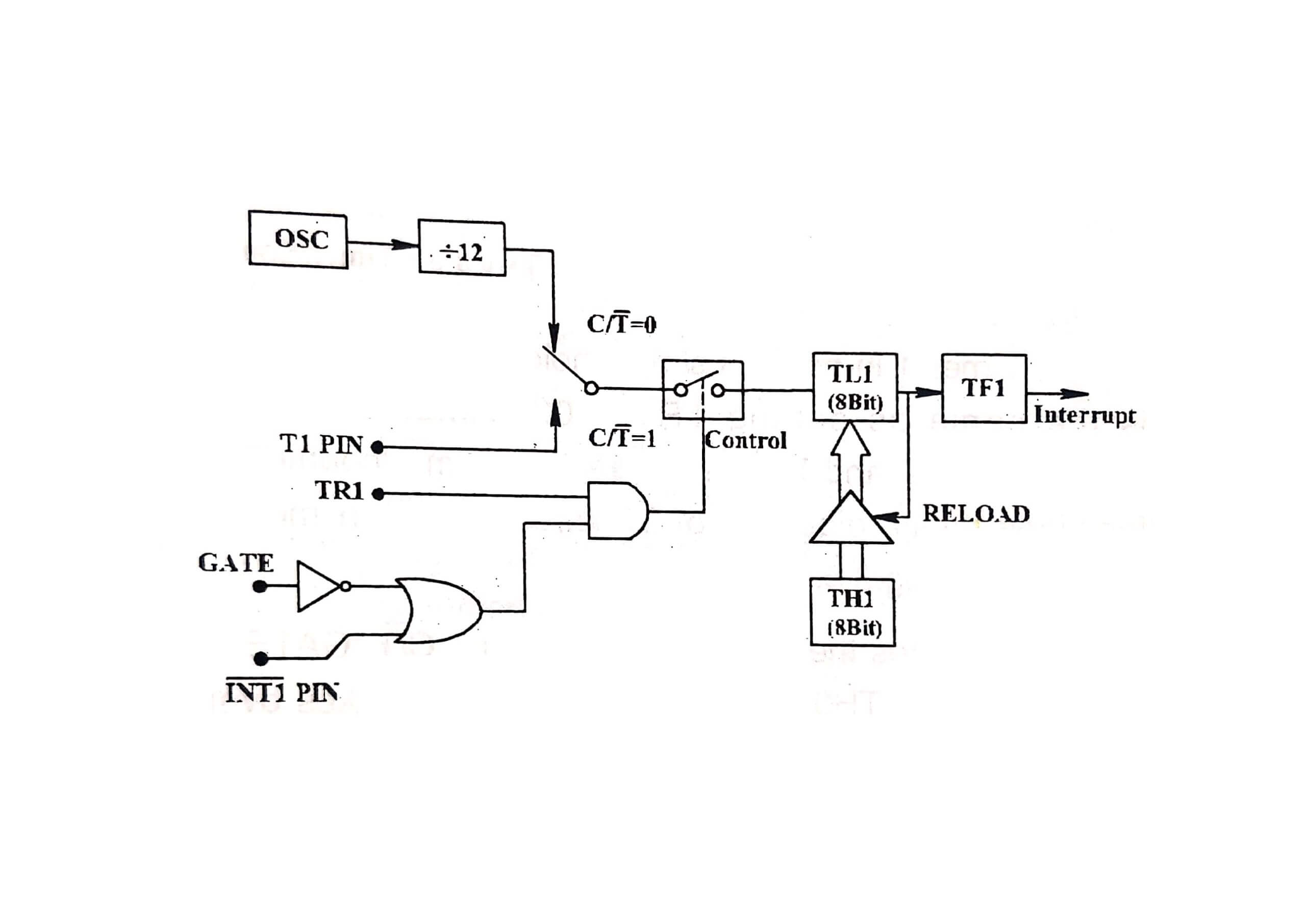
Microcontroller 8051 has two 16-bit timer / counter registers. They are timer 0 and timer 1. Both can configured to operate either as timers or event counters. In the timer function, the register is incremented every machine cycle. That means, in timer operation it counts the machine cycles. Since a machine cycle consists of 12 oscillator periods, the count rate is 1/12 of the oscillator frequency (fosc/12).
In the counter function, the register is incremented in response to “1 to O” transition at its corresponding external input pin TO or T1. In this function the external input is sampled during S5P2 of every machine cycle. When the samples show a high in one machine cycle and a low in the next machine cycle, the count is incremented. The new count value appears in the register during S3P1 of the cycle following the one in which the transition was detected. Since it takes atleast 2 machine cycles (24 oscillator periods) to recognize a “1 to o” transition. The maximum count rate is 1/24 of the oscillator frequency (fosc/24).
In addition to the timer or counter selection, Timer 0 and Timer have four operating modes. The timer/counters are divided into two 8-bit registers called the timer low (THO, TL0) and timer high (TH1, TL1) bytes.
All timer/counter actions are controlled by bit status in the timer mode control register (TMOD), the timer /counter control register (TCON) and certain program instructions.


