Interfacing Microcontroller 8225
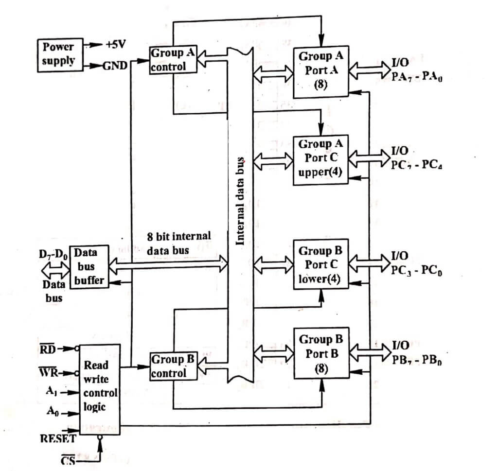
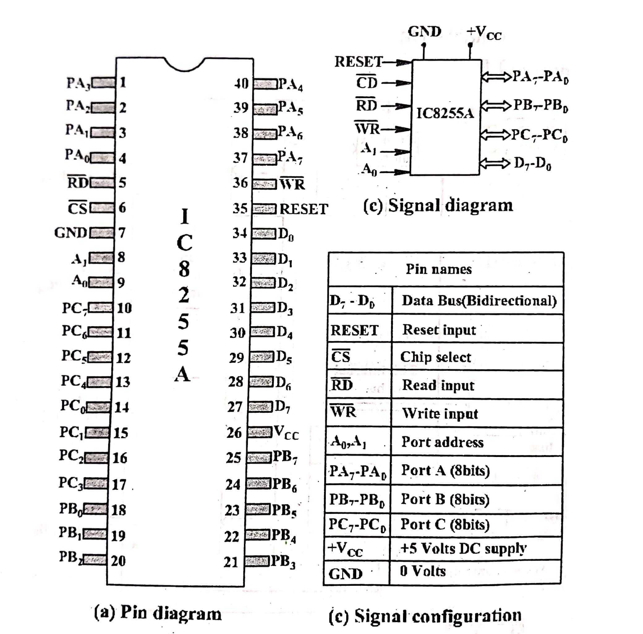
The INTEL 8255 is a general purpose programmable peripheral interface. It is used to perform a variety of input/output functions in a microcomputer system. It is a 40 pin DIP IC. It requires +5V DC power supply for its operations. The 8255 Interfacing the microprocessor/ microcontroller on one side with peripherals on the other side. The functional block diagram of 8255 is shown in the image. It contains data bus buffer, Read/ write control logic unit and I/O ports.
Input/output Ports – Interfacing
The 8255 consists of two 8-bit ports of Port A and Port B, and two 4-bits ports of Port C upper (CU) and Port C lower (CL). For the convenience of programming, the Ports are grouped as Group A and Group B. Group A consists of Port A (PA7 – PAO) and Port C upper ( PC7 – PC4). Group B consists of Port B (PB7 – PB0) and Port C lower (PC3 – PCO).
Data bus buffer – Interfacing Microcontroller 8225
It is a bidirectional 8-bit buffer. It is used to interface the 8255 with the system data bus. The data, control word and status information signal in between the microcontroller and 8255 are communicated only through data bus buffer.
Control logic
The read/write control logic unit has 6 control signals. These signals are given below;
RD (Read) : When this. signal is low, the micro processor/ interfacing microcontroller reads data from the selected 1/0 port of 8255.
WR (Write) : When this signal is low, the microprocessor/ microcontroller writes data into the selected I/O port or the control register.
RESET : It is an active high signal. When it is high, it clears the control word register and sets all ports in the input mode.
CS (Chip select) :It is an active low signal. It enables the communication between the 8255 and the microprocessor/ microcontroller.
A, – A0 : These lines are used for selecting the ports or control word register of 8255 as shown in the table. These lines. are generally connected to the micro processor/microcontroller address lines.
Control word – Interfacing Microcontroller 8225
The control section of 8255 has an 8-bit register called control register. An 8-bit binary word present in the control register is called control word. The control word specifies the function for each I/O port.
Various modes of operations
The operation of 8255 can be classified into two modes. They are Bit Set/Reset (BSR) mode and 1/0 mode. The Bit D7 of the control word determines either the 1/0 function or the BSR function.
I/O mode – Interfacing
The I/0 mode is further classified into three modes.
They are
Mode 0 – Simple I/O Port
Mode 1 – Strobed I/O Port (Hand shake I/O Port)
Mode 2 – Bidirectional 1/0 Port
Mode 1 (Strobed I/O port)
In this mode ports A and B can be programmed as input port or output port. In this mode hand either shake signals are exchanged between the controller and peripherals to data transfer. The port C pins are used prior for handshake signals.
Mode 1 Input configuration
Port A – Input port
PC3 – PC5 : – Control signals for port A
Port B – Input port
PC0 – PC2 :- Control signals for port B
PC6, PC7 : – Not used, they can be used in Mode 0
(A simple I/O pins)
The details of control signals are explained below
- STB (Strobe) It is an active low signal, generated by a peripheral device, to indicate that it has to be transmitted a byte of data.
- IBF (Input Buffer Full) It is an active high acknowledge signal, generated by 8255, to indicate that the input latch has received a data byte.
- INTR (Interrupt Request) It is an active high signal, used to interrupt the controller, when its input buffer is full. The representation of input a Tone: configuration in Mode 1 is shown in the image.
In this mode port A only acts as bidirectional data transfer port. Port A uses five signals from Port C as control signals for data transfer. The remaining bits from Port C can be used in mode 0 or as may be operated as in handshake signals for Port B. Port B mode 0 or mode 1.
In this mode the data transfer is done in both directions, in between the microcontroller and peripheral devices. The configuration of mode 2 is shown in the image

Bit Set/Reset Mode (BSR Mode)
This mode is related to only Port C. The bits of Port C can be controlled directly by the microcontroller. word with bit D7 = 0, is called a BSR control word. Using this bit set-reset feature, the microcontroller can send a command to 8255 for setting/resetting the bits of port C. The control word format for BSR mode is the image.
Advantages
The advantage of I/0 port expansion is that the entire range of 8051 instruction can be used to access the added ports.
Disadvantages
The expanding 10 ports will reduce the speed of operation, because it takes extra time to write control bits to ports, before the resulting I/O ports can be accessed.
INTERFACING TECHNIQUES – Introduction
In a microcontroller system, the microcontroller accepts data from input devices such as key board, switches and A/D converters. Then it processes the data as per the instructions received from the memory unit. After processing the data, it sends the result to the output devices, such as seven segment LED display, D/A converters, printers and video monitors. These input and output devices are called peripherals. Memory is also a special type of peripheral interfacing.
In many cases, it may not be possible to connect the peripherals directly to the microcontroller. Designing logic circuits and writing instructions to enable the microcontroller/ microprocessor to communicate with these peripherals is called interfacing. The logic circuits are called interfacing devices.
Interfacing external memory to 8051
The microcontroller 8051 has separate address spaces for program storage and data storage. Depending on the type of instructions, the same address can refer to two logically and physically different memory spaces.
The bidirectional data bus DO-D7 of 8255 is directly connected to port 0 of 8051. Address latch 74LS373 is used to demultiplex the lower order 8-bits of the address bus from multiplexed address/data bus AD0-AD7 (P0.0 – PO.7).
The control lines WR and RD are directly connected to the WR and RD lines of 8051. The 8255 is connected to the 8051 by using memory mapped 1/0 scheme. Hence the Separate 8255 is treated as external data memory. addresses are assigned to Port A, Port B, Port C and control By using the instruction the word register. MOVX microcontroller can access the ports and CWR of 8255.
Relays
A relay is an electrically controllable switch widely used in industrial controls, automobiles and appliances. It allows the isolation of two separate sections of a system with two sources. The electromagnetic have different voltage relays three components: the coil, spring and contacts. When current flows through a coil, a magnetic field is created around the coil, the coll is energized which causes the armature to be attracted to the coil. The armature’s contact acts like a switch and closes the normally open contact and opens the normally closed contact. When the coil is not energized, the spring pulls the armature to its normal state of open or closed.
Driving a relay
Digital system and microcontroller pins could not produce sufficient current to drive the relay. While relay’s coil needs around 10mA current to be energized, the microcontroller’s pin can provide a maximum of 1-2mA current. For this reason, we place a driver or a power transistor in between the microcontroller and the relay.
An opto isolator has an LED transmitter and a photo sensor receiver, both are separated from each other by a small gap. When current flows through the LED, it transmits a light signal to the receiver. The receiver produces the signal with the same phase but a different current and amplitude.
Opto isolators are also widely used in communication equipment such as modems. This allows a computer to be connected to a telephone line without risk of damage from power surges.
The gap between the transmitter and receiver of isolators prevents the electrical current surge from reaching the system.
ADC interfacing
Analog to Digital converters are most widely used devices for data acquistion. Digital computers use binary (discrete) values, but in the physical world everything is analog (continuous). Temperature, pressure, humidity, and velocity are few examples of physical quantities. A physical quantity is converted into electrical signals (voltage or current) by using a device called a transducer. Transducers are also referred to as sensors. lam Bys
An ADC has n-bit resolution where “n” can be 8, 10, 12, 16 or even 24 bits. The higher resolution ADC provides a smaller step size. The conversion time of ADC is defined as the time it takes the ADC to convert the analog input to digital number. The ADC chips are either parallel or serial. In parallel ADC, 8 or more pins are provided for bringing out the binary data; but in serial ADC only one pin is provided for bringing the binary data (digital)


