Bipolar junction transistors generally comprise n-p-n or p-n-p junctions of either silicon (Si) or germanium (Ge) material. The junctions are, in fact, produced in a single slice of silicon by diffusing impurities through a photographically reduced mask. Silicon transistors are superior when compared with germanium transistors in the vast majority of applications (particularly at high temperatures) and thus germanium devices are very rarely encountered in modern electronic equipment.
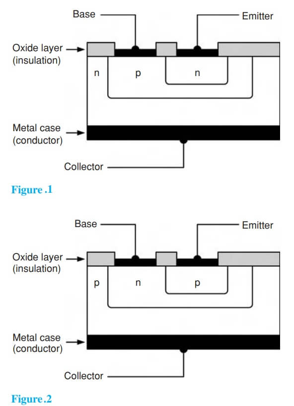
The construction of typical n-p-n and p-n-p transistors is shown in Figs.1 and 2. In order to conduct the heat away from the junction (important in medium- and high-power applications) the collector is connected to the metal case of the transistor.
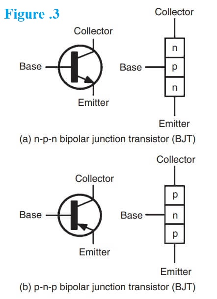
The symbols and simplified junction models for n-p-n and p-n-p transistors are shown in Fig. 3. It is important to note that the base region (p-type material in the case of an n-p-n transistor or n-type material in the case of a p-n-p transistor) is extremely narrow.
| Read More Topics |
| Conduction in semiconductor materials |
| Introduction to electromagnetic induction |
| Force on a current carrying conductor |
| Magnetic field due to an electric current |

