Structures for InGaAs
To improve the performance of structures for InGaAs APDs, various complex device architectures have been devised. One widely used structure is the separate-absorption-and-multiplication (SAM) APD configuration.
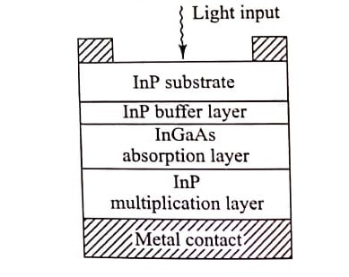
Image shows, this structure uses different materials in the absorption and multiplication regions, with each region being optimized for a particular function. Here, light enters the APD through the InP substrate. Since this material has a larger energy band-gap, it allows long-wavelength photons to pass through to the InGaAs absorption region where electron-hole pairs are generated.
Following this is an InP layer that is used for the multiplication region because high electric fields needed for the gain mechanism can exist in InP without tunneling breakdown. This device structure gets its name SAM as a result of the separation of the absorption and multiplication regions.
- Variations on the SAM structure include adding other layers to the device.
- Using a grading layer between the absorption and multiplication regions to increase the response time and bandwidth of the device.
- Adding a charge layer that provides better control of the electric field profile.
- Incorporating a resonant cavity that decouples the optical and electrical path lengths to achieve high quantum efficiencies and wide bandwidths simul-taneously.
Another popular design for InGaAs APDs is the superlattice structure. In these devices, the multiplication region is around 250 nm thick and consists of, for example, 13 layers of 9-nm-thick InAIGaAs quantum wells separated by 12-nm-thick InAlAs barrier layers. This structure improves the speed and sensitivity of InGaAs APDs, thereby allowing them to be used for applications such as 10-Gb/s long-distance systems (e.g., SONET OC-192/SDH STM-64 links).
- The transit time of the photocarriers in the depletion region.
- The diffusion time of the photocarriers generated outside the depletion region.
- The RC time constant of the photodiode and its associated circuit.
- See More : Point to point links optical
- See More : Radio over fiber links
- See More : Reactive power and voltage control
- See More : Power system security analysis


