A basic understanding of the fabrication technology for integrated circuit, which precedes that of MEMS in history, is necessary to understanding the micromachining process. A reader who is familiar with the basic microfabrication process of integrated circuits may skip this section.
A fabrication process for integrated circuits generally involves many steps of material deposition, material removal, and patterning, as illustrated in the following example.
A generic microfabrication process for realizing a field effect transistor, the building block of modern integrated circuits, is illustrated in figure. By repeating the cycle of deposition-lithography-etching, devices with arbitrary complexity can be built.
In this particular case, six major cycles transforms a bare silicon wafer to one with a metal-oxide-semiconductor (MOS) field effect transistor (FET) on the front surface.
The figure depicts 30 major steps, showing cross-sectional view at a single FET level. Steps 1.0, 2.0, 3.0, 4.0, 5.0, 6.0, 7.0, and 8.0, on the left most column, are major milestones in the process, whereas process steps x.y (x = 1 – 7, y ≠ 0), are steps that leads to the next major milestone.
The nature of each step is clearly marked. Letters D, L, E, and M denotes deposition, lithography (photo exposure and development), etching, and modification/treatment of materials.
A brief description of each step is presented below:
Step 1.0. The figure depicts the cross section of a starting bare silicon wafer. The wafer thickness is not drawn to scale. Material process steps occurring on the backside of a wafer are not drawn in future steps for the sake of simplicity.
Step 2.0. A layer of oxide is deposited. The oxide is patterned using the following subsequent steps (2.1 through 2.3). This oxide layer is here only to serve a transitional purpose. (This point will become obvious later.)
2.1. A photosensitive resist layer is deposited on top of the oxide by spin coating.
2.2. The photosensitive resist is lithographically exposed and developed.
2.3. The photoresist is used as a mask for etching the oxide.
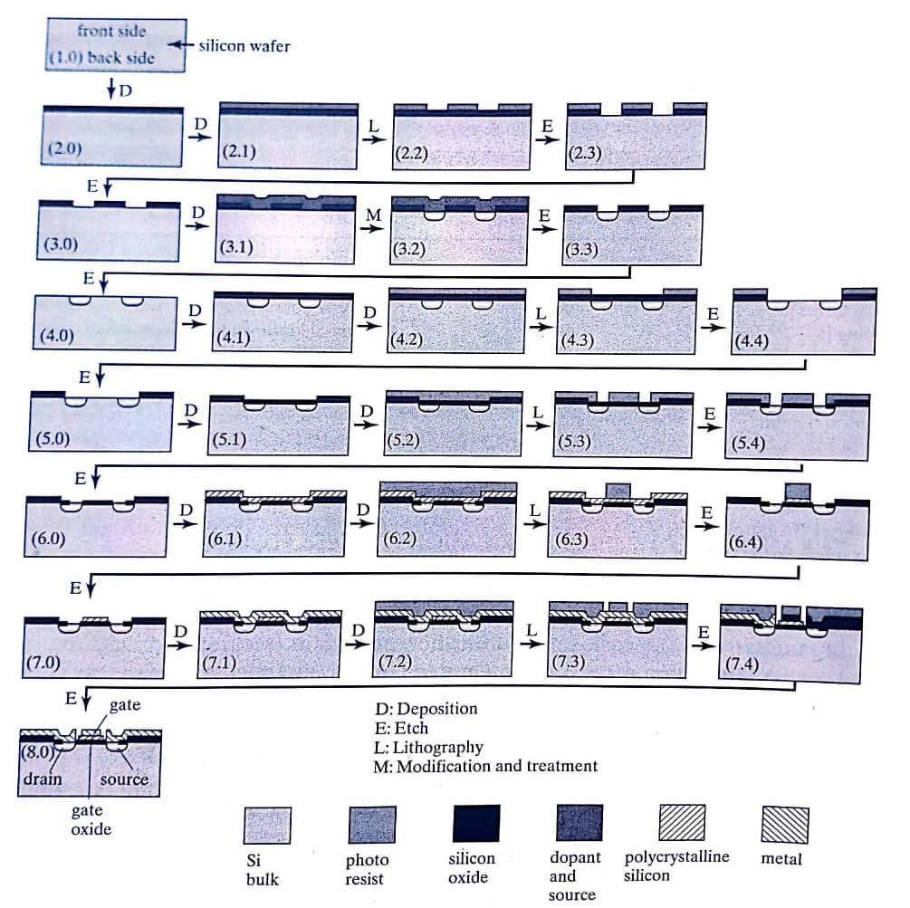
Step 3.0. The photoresist is removed using organic solvents. The patterned oxide is used as a mask against impurity doping performed in step 3.1 through 3.3.
3.1. A layer of material containing dopant impurities is deposited.
3.2. The wafer is thermally treated, causing the dopant to diffuse into silicon in areas not covered by the oxide.
3.3. The dopant-source layer deposited in step 3.1 is removed.
Step 4.0. The oxide is removed. Note that many steps and layers of materials are involved to transform a bare wafer (step 1.0) to a wafer with dopant in selective places (step 4.0).
Additional processes (steps 4.1 through 4.4) are then performed to produce another layer of patterned oxide.
4.1. Another layer of silicon oxide is grown.
4.2. A photosensitive resist is deposited.
4.3. The resist is lithographically patterned.
4.4. Using the resist as a mask, the oxide is etched.
Step 5.0. The resist deposited in step 4.2 is removed. From Step 4.0 to 5.0, the major difference is oxide cover in undoped regions. An oxide layer is then deposited and patterned (5.1. through 5.4).
5.1. A very thin oxide is grown. This so-called gate oxide layer must have very high quality and are free of contaminants and defects.
5.2. A resist layer is again deposited.
5.3. The resist is lithographically patterned.
5.4. The resist serves as a mask for selectively etching the gate oxide.
Step 6.0. The resist deposited in step 5.2 is removed. The active regions not covered by oxide will provide electrical contact to metal. A gate electrode, made of polycrystalline silicon, is then deposited and patterned in steps 6.1 through 6.4.
6.1. A layer of polycrystalline (doped) silicon is deposited.
6.2. A layer of photosensitive resist is deposited.
6.3. The resist is patterned lithographically.
6.4. The resist serves as a mask for etching the underlying polycrystalline silicon selectively.
Step 7.0. The resist is removed by using organic solvents. The difference between steps 6.0 to 7.0 is the addition of polycrystalline silicon. Each transistor must be connected with each other and to the outside through low-resistivity metal wires. The metal wires are made in steps 7.1 through 7.3.
7.1. A layer of metal is deposited.
7.2. and 7.3. The metal is coated with resist and lithographically patterned.
7.4. The resist serves as a mask for etching the metal.
Step 8.0. The resist is removed, realizing a complete field effector transistor.
The process used in the industry follows the basic flow diagramed in figure but involves more detailed steps for quality assurance, functional enhancement, and for increasing the yield and repeatability. Many more steps may incur alter step 8.0 as well. A complete process run from the start to the finish may take 3 months, and 20-40 mask plates.
| Read More Topics |
| Plasma etching & reactive ion etching |
| Vibration galvanometer |
| Duddell’s oscillograph element |
| Standards of mutual inductance |
