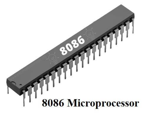
A 40 pin DIP Intel 8086 microprocessor is shown in image. 8086 microprocessor can operate in two modes. Minimum mode and maximum mode. The pins 24 to 31 have alternate functions for every mode.

- The 8086 is a 16 bit Microprocessor.
- Intel 8086 has a 16 bit Data bus.
- The 8086 has a 20 bit Address bus.
- Direct addressing capability 1 M Byte of Memory (27°).
- It provides fourteen 16-bit register.
- 24 Operand addressing modes.
- Bit, Byte, Word, and Block operations
- 8 and 16-bit Signed and Unsigned arithmetic operations including multiply and Divide.
- Four general-purpose 16-bit registers: AX, BX, CX, DX
- Two Pointer group registers: Stack Pointer (SP), Base Pointer (BP)
- Two Index group registers: Source Index (SI), Destination Index (DI
- Four Segment registers: Code Segment (CS), Data Segment (DS), Stack Segment
- (SS), Extra Segment (ES).
- 6 status flags and 3 control flags.
- Memory is byte-addressable”-each address stores an 8-bit value.
- Addresses can be up to 32 bits long, resulting in up to 4 GB of memory
- Range of clock rates: 5 MHz for 8086, 8 MHz for 8086-2, 10 MHz for 8086-1
- Multibus system compatible interface
- Available in 40pin Plastic Package and Lead Cerdip.
Intel 8086 Architecture
- The internal functions of the 8086 microprocessor are partitioned logically into two processing.
- Architecture of 8086
- Bus Interface Unit (BIU)
- Execution Unit (EU)
The BIU and EU function independently. BIU interfaces the 8086 to the outside world. The BIU fetches instructions, reads data from memory and ports, and writes data memory and I/O ports. EU (Execution Unit) receives program instruction codes and data from the BIU, execute these instructions and stores the results either in the general registers or output them through the BIU. EU has no connections to the system buses. It receives and outputs all

The BIU contains:
- Segment registers
- Instruction pointer
- Instruction queue
The EU contains:
- ALU
- General purpose registers
- Index registers
- Pointers
- Flag Register
- General Purpose Registers
All general registers of the 8086 microprocessor can be used for arithmetic and logic operations. The 16 bit general registers are:
- Accumulator register (AX)
- Base register (BX)
- Count register (CX)
- Data register (DX)
(i) Accumulator register
It consist of two 8 bits registers AL and AH, which can be combined and used together as 16 bit registers AX . AL contains the lower order byte of the word and AH contains the higher order byte of the word. Accumulator can be used for I/O operations.
(ii) Base register
It consists of two 8-bit registers BL and BH, which can be combined together and used as 16-bit registers BX. . BL contains the lower order byte of the word and BH contains the higher order byte of the word. BX register usually contains a data pointer used for based, based indexed or register indirect addressing.
(iii) Count register
It consists of two 8-bit registers CL and CH, which can be combined together and used as a 16-bit register CX. When combined, CL register contains the low-order byte of the word, and CH contains the high-order byte. Count register can be used as a counter in string manipulation and shift/rotate instructions.
(iv) Data register
It consists of two 8-bit registers DL and DH, which can be combined together and used as a 16-bit register DX. When combined, DL register contains the low-order byte of the word and DH contains the higher order byte. Data register can be used as a port number in I/O operations. In integer 32-bit multiply and divide instruction the DX register contains high order word of the initial or resulting number.
Segment Registers
Most of the registers contain data/in for instructions, offsets within 64 KB memory segment.
There are four different 64 KB segments segment registers are:
- Code segment (CS)
- Stack segment (SS)
- Data segment (DS)
- Extra segment (ES)
It is a 16-bit register containing address of 64 KB segment with processor instructions, The processor uses CS register for all accesses to instructions IP register. CS register cannot be changed directly. The CS register is automatically updated during FAR JUMP, FAR CALL and FAR RET instructions.
(ii) Stack segment (SS)
It is a 16-bit register containing address of 64KB segment with program stack. By default, the processor assumes that all data referenced by the stack pointer (SP) and base pointer (BP) registers are located in the stack segment .SS register can be changed directly using POP instruction.
(iii) Data segment (DS)
It is a 16-bit register containing address of 64KB segment with program data. By default, the processor assumes that all data referenced by general registers (AX, BX, Cx,DX) and index register (SI, DI) is located in the data segment. DS register can be changed directly using POP and LDS instructions
(iv) Extra segment (ES)
It isa 16-bit register containing address of 64KB segment, usually with program data. By default, the microprocessor assumes that the DI register references the ES segment in string manipulation instructions. ES register can be changed directly using POP and LES instructions. It is possible to change default segments used by general index registers by prefixing instructions with a CS, SS, DS or ES prefix.
Pointer Registers
(i) Stack Pointer (SP)
It is a 16-bit register pointing to program stack.
(ii) Base Pointer (BP)
It is a 16-bit register pointing to data in the stack segment for based, based indexed or register indirect addressing
Index Registers
(i) Source Index (SI)
It is a 16-bit register. SI] is used for indexed, based indexed and register indirect addressing, as well as a source data address in string manipulation instructions, Intel 8086 Microprocessor.
(ii) Destination Index (DI)
It is a 16-bit register. DI is used for indexed, based indexed and register indirect addressing, as well as a destination data address in string manipulation instructions.
Instruction Pointer (IP)
It is a 16-bit register. The operation is same as the program counter. The IP register is updated by the BIU to point to the address of the next instruction. Programs do not have direct access to the IP, but during execution of a program the can be modified or saved and restored from the stack.
Flag Register
It is a 16-bit register containing nine 1-bit flags: Six status or condition flags (OF, SF, ZF, AF, PF, CF) Three control flags ( TF, DF, IF)
- Overflow Flag (OF) – set if the result is too large positive number, or is too small negative number to fit into destination operand.
- Sign Flag (SF) – set if the most significant bit of the result is set.
- Zero Flag (ZF) – set if the result is zero.
- Auxiliary carry Flag (AF) – set if there was a carry from or borrow to bits 0-3 in the AL register.
- Parity Flag (PF) – set if parity in the low-order byte of the result is even.
- Carry Flag (CF) – set if there was a carry from or borrow to the most significant bit during last result calculation
- Trap or Single-step Flag (TF) – if set then single-step interrupt will occur after the next instruction.
- Direction Flag (DF) – if set then string manipulation instructions will auto-decrement index registers. If cleared then the index registers will be auto-incremented
- Interrupt-enable Flag (IF) – setting this bit enables maskable interrupts.
- AH AL Accumulator (AX)
- BH BL Base (BX)
- CH CL Count (CX)
- DH DL Data _ (DX)
- SP Stack Pointer
- BP Base Pointer
- SI Source Index
- DI Destination Index
- CS Code Segment
- _DS Data Segment
- SS Source Segment
- ES Extra Segment
- IP Instruction Pointer
- Instruction Queue
The instruction queue is a First-In-First-out (FIFO) group of registers where 6 bytes of instruction code is pre-fetched from memory ahead of time. It is being done to speed-up program execution by overlapping instruction fetch and execution. This mechanism is known as PIPELINING, If the queue is full, the BIU does not perform any bus cycle.
BIU is not full and can store at least 2 bytes and EU does not request to access its memory the BIU may pre-fetch instructions
If the BIU is interrupted by the EU for memory access while pre-fetching, the BIU first completes fetching and then services the EU. In case of JMP instruction, the BIU will reset the queue and begin refilling after Passing the new instruction to the EU.
ALU:
It is a 16 bit register. It can add, subtract, Increment, decrement complement, shift numbers and performs AND, OR, XOR Operations
Control unit:
The control units in EU directs the internal operations like RD,WR,M/IO
Instruction set
8086 instruction set consists of the following instructions
- Data moving instructions.
- Arithmetic instructions – add, subtract, increment, decrement, convert byte/word and compare.
- Logic instructions – AND, OR, exclusive OR, shift/rotate and test
- String manipulation instructions – load, store, move, compare and scan for byte/ word.
- Control transfer instructions – conditional, unconditional, call subroutine and return from subroutine
- Input/Output instructions – Intel 8086 Microprocessor
- Other instructions – setting/clearing flag bits, stack operations, software interrupts,etc.
Addressing modes
Implied – the data value/data address is implicitly associated with the instruction.
Register – references the data in a register or in a register pair..
Immediate – the data is provided in the instruction.
Direct – the instruction operand specifies the memory address where data is located.
Register indirect – instruction specifies a register-containing an address, where data is located. This addressing mode works with SI, DI, BX and BP registers.
Based – 8-bit or 16-bit instruction operand is added to the contents of a base register (BX or BP), the resulting value is a pointer to location where data resides.
Indexed – 8-bit or 16-bit instruction operand is added to the contents of an index register (SI or DI), the resulting value is a pointer to location where data resides.
Based Indexed – the contents of a base register (BX or BP) is added to the contents of an index register (SI or DI), the resulting value is a pointer to location where data resides.
Based Indexed with displacement – 8-bit or 16-bit instruction operand is added to the contents of a base register (BX or BP) and index register (SI or DI), the resulting value is a Pointer to location where data resides.
Interrupts
The 8086 microprocessor has the following interrupts: INTR is a maskable hardware interrupt. The interrupt can be enabled/disabled using STI/CL] instructions or using more complicated method of updating the FLAGS register With the help of the POPF instruction. When an interrupt occurs, the processor stores FLAGS” register into stack, disables further interrupts, fetches from the bus one byte representing interrupt type, and jumps to interrupt processing routine address of which 1s stored in location <interrupt type>. Interrupt processing routine should return with the IRET instruction.
NMI is a non-maskable interrupt. Interrupt is processed in the same way as the INTR interrupt. Interrupt type of the NMI is 2, i.e. the address of the NMI processing routine stored in location 0008 H. This interrupt has higher priority then the maskable Interrupt,
Software interrupts can be caused by :
- INT instruction – breakpoint interrupt. This is a type 3 interrupt.
- INT <interrupt number> instruction – any one interrupt from available 25, interrupts.
- INTO instruction – interrupt on overflow
- Single-step interrupt – generated if the TF flag is set. This is a type | interrupt, When the CPU microprocesses this interrupt it clears TF flag before calling the interrupt processing routine. Software interrupt processing is the same as for the hardware interrupts.
Read RD
This signal is used to read data from memory or I/O device which reside on the 8086 local bus. microprocessor
Ready
If this signal is low the 8086 enters into WAIT state. The READY signal from memory/IO is synchronized by the 8284A clock generator to form READY. This signal is active HIGH. ,
Interrupt Request (INTR)
It is a level triggered maskable interrupt request. A subroutine is vectored via an interrupt vector lookup table located in system memory. It can be internally masked by software resetting the interrupt enable bit. INTR is internally synchronized. This signal is active HIGH.
Test
This input is examined by the “Wait” instruction. If the TEST input is LOW execution continues, otherwise the microprocessor waits in an “Idle” state. This input is synchronized internally during each clock cycle on the leading edge of CLK.
Non-Maskable Interrupt (NMI)
It is an edge triggered input which causes a type 2 interrupt. NMI is not maskable internally by software. A transition from LOW to HIGH initiates the interrupt at the end of the current instruction.
Reset
This signal is used to reset the 8086. It causes the processor to immediately terminate its present activity The signal must be active HIGH for at least four clock cycles It restarts execution when RESET returns LOW
Clock CLK
This signal provides the basic timing for the processor and bus controller. The clock frequency may be 5 MHz or 8 MHz or 10 MHz depending on the version of 8086
Ground (GND)
Two pins (1 and 20) are connected .to ground ie, 0 V power supply.
Minimum/Maximum (MN/ Mx)
This pin indicates what mode the processor is to operate in. The 8086 can be configured in either minimum mode or maximum mode using this pin
Minimum Mode Signals: MEMORY / IO (M/IO)
It is used to distinguish a memory access from an I/O access.. M = HIGH, I/O = LOW.
WRITE( WR)
It indicates that the microprocessor is performing a write memory or write I/O cycle, depending on the state of the i/o signal.
Interrupt Acknowledge (INTA)
This signal indicates recognition of an interrupt request. It is used as a read strobe for interrupt acknowledge cycles.
Address Latch Enable (ALE)
This signal is used to demultiplex ADo AD15 into Ao A15 and Do D15 its high pulse active during any T1 of any bus cycle
Data Transmit/Receive (DT/R)
This signal desires to use a data bus transceiver (8286/8287), It is used to control the direction of data flow through the transceiver. A high signal on this pin indicates that 8086’S transmitting the data and low indicates that 8086 is receiving the data.
Program memory – Intel 8086 Microprocessor
The program can be located anywhere in memory. Jump and call instructions can bused for short jumps within currently selected 64 KB code segment, as well as for far jumps anywhere within | MB of memory. All conditional jump instructions can be used to jump within approximately +127 to -127 bytes from current instruction.
Data memory earner
The processor can access data in any one out of 4 available segments, which limits the size of accessible memory to 256 KB (if all four segments point to different 64 KB blocks).
Accessing data from the Data, Code, Stack or Extra segments can be usually done by prefixing the instructions with DS:, CS:, SS: or ES: (some registers and instructions by default may use the ES or SS segment instead of DS segment).
Word data can be located at odd or even byte boundaries. The processors uses two, memory accesses to read 16-bit word located at odd byte boundaries. Reading Word data from even byte boundaries requires only one memory access.
Stack memory
It can be placed anywhere in memory. The stack can be located at odd memory addresses but it is not recommended for performance reasons Intel 8086 Microprocessor.
Addressing Modes – 8086 Microprocessor
An addressing mode is the way the 8086 identifies the operands for the instruction. A},instructions that access the data use one or more of the addressing modes. The memory address of an operand consists of two component Starting address of the memory segment
Offset
The 16 MSBs of the starting address of the memory segment resides in the corresponding segment register. When an operand is stored in a memory location, how for the operand memory location is within a memory segment from the starting address of the segment, is called Offset or Effective Address (EA). An offset is determined by adding any combination of three address elements: Displacement, Base or Index. The combination depends on the addressing mode of the instruction.
Displacement: It is the content of the index register, SI or DI The 8086 uses 20 bit memory address. The segment register gives 16 MSBs of the starting address of the memory segment. The BIU generates 20 bit starting address of the memory segment by shifting the content of the segment register left by 4 bits. In other words it puts 4 zeros in 4 LSB positions Intel 8086 Microprocessor
Displacement : It is an 8-bit or 16-bit immediate value given in the instruction
Base: It is the content of the base register, BX or BP
Index: It is the content of the Index register, SI or DI
The Intel 8086 Microprocessor has the following addressing modes:
- Register Addressing Mode
- Immediate Addressing Mode
- Direct Addressing Mode
- Register Indirect Addressing Mode
- Base Addressing Mode
- Indexed Addressing Mode
| Read More Topics |
| Components of control system |
| Microprocess based controller |
| Instruction set architecture 8051 |
| Multiprocessor configuration of 8086 |