Introduction Avalanche Photodiode
At the output end of an optical transmission line, avalanche photodiode there must be a receiving device which interprets the information contained in the optical signal. The first element of this receiver is a photodetector.
The photodetector senses the luminescent power falling upon it and converts the variation of this optical power into a correspondingly varying electric current.
Since the optical signal is generally weakened and distorted when it emerges from the end of the fiber, the photodetector must meet very high performance requirements.
Among the foremost of these requirements are a high response or sensitivity in the emission wavelength range of the optical source being used, a minimum addition of noise to the system, and fast response speed or sufficient bandwidth to handle the desired data rate.
The photodetector should also be insensitive to variations in temperature, be compatible with the physical dimensions of the optical fiber, have a reasonable cost in relation to the other components of the system, and have a long operating life.
Several different types of photodetectors are in existence. Among these are photomultipliers, pyroelectric detectors, and semiconductor-based photoconductors, phototransistors, and avalanche photodiode However, many of these detectors do not meet one or more of the foregoing requirements.
Photomultipliers consisting of a photocathode and an electron multiplier packaged in a vacuum tube are capable of very high gain and very low noise.
Unfortunately, their large size and high voltage requirements make them unsuitable for optical fiber systems. Pyroelectric photodetectors involve the conversion of photons to heat.
Photon absorption results in a temperature change of the detector material. This gives rise to a variation in the dielectric constant which is usually measured as a capacitance change.
The response of this detector is quite flat over a broad spectral band, but its speed is limited by the detector cooling rate after it has been excited. Its principal use is for detecting high-speed laser pulses, and it is not well suited for optical fiber systems.

Physical Principles of Avalanche Photodiode
Of the semiconductor-based photodetectors, the photodiode is used almost exclusively for fiber optic systems because of its small size, suitable material, high sensitivity, and fast response time.
The two types of photodiodes used are the pin photodetector and the avalanche photodiode (APD). We shall examine the fundamental characteristics of these two device types in the following sections.
In describing these components, we shall make use of the elementary principles of semiconductor device physics given in before Basic discussions of photodetection processes can be found in various texts.
The pin Photodetector
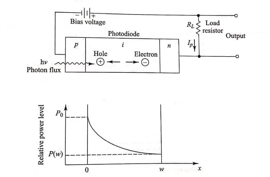
The most common semiconductor photodetector is the pin photodiode, shown schematically in heading image. The device structure consists of p and n regions separated by a very lightly n-doped intrinsic region.
In normal operation a sufficiently large reverse bias voltage is applied across the device so that the intrinsic region is fully depleted of carriers.
That is, the intrinsic n and p carrier concentrations are negligibly small in comparison with the imprison with the impurity concentration in this region.
Representation of a pin photodiode circuit with an applied reverse bias. An incident optical power level decays exponentially inside the device
When an incident photon has an energy greater than or equal to the band-gap energy of the semiconductor material, the photon can give up its energy and excite an electron from the valance band to the conduction band.
This process generates mobile electron-hole pairs, These electrons and holes are known as photocarriers, since they are photon-generated charge carriers that are available to produce a current flow when a bias voltage is applied across the device.
The number of charge carriers is controlled by the concentration level of impurity elements that are intentionally added to the material.
The photodetector amplifiers is normally designed so that these carriers are generated mainly in the depletion region (the depleted intrinsic region) where most of the incident light is absorbed.
The high electric field present in the depletion region causes the carriers to separate and be collected across the reverse-biased junction.
This gives rise to a current flow in an external circuit, with one electron flowing for every carrier pair generated. This current flow is known as the photocurrent.
As the charge carriers flow through the material, some electron-hole pairs will recombine and hence disappear. On the average, the charge carriers move a distance Ln or Lp, for electrons and holes, respectively.
Avalanche Photodiodes
Avalanche photodiodes (APDs) internally multiply the primary signal photocurrent before it enters the input circuitry of the following amplifier.
This increases receiver sensitivity, since the photocurrent is multiplied before encountering the thermal noise associated with the receiver circuit.
In order for carrier multiplication to take place, the photogenerated carriers must traverse a region where a very high electric field is present.
In this high-field region, a photogenerated electron or hole can gain enough energy so that it ionizes bound electrons in the valence band upon colliding with them.
This carrier multiplication mechanism is known as impact ionization.
The newly created carriers are also accelerated by the high electric field, thus gaining enough energy to cause further impact ionization.
This phenomenon is the avalanche effect. Below the diode breakdown voltage a finite total number of carriers are created, whereas above breakdown the number can be infinite.
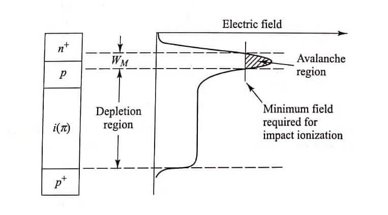
A commonly used structure for achieving carrier multiplication with very little excess noise is the reach through construction 14-16 shown in blow image.
The reach-through avalanche photodiode (RAPD) is composed of a high-resistivity p-type material deposited as an epitaxial layer on a pt (heavily doped p-type) substrate.
A p-type diffusion or ion implant is then made in the high-resistivity material, followed by the construction of an nt (heavily doped n-type) layer.
For silicon, the dopants used to form these layers are normally boron and phosphorus, respectively. This configuration is referred to as p+ πpn+ reach-through structure.
The 7 layer is basically an intrinsic material that inadvertently has some p doping because of imperfect purification. blow describes more complex structures used for InGaAs APDs.

Reach-through avalanche photodiode structure and the electric fields in the depletion and multiplication regions
Photodetector Noise – Optical Fiber Communication
In fiber optic communication systems, the photodiode is generally required to detect very weak optical signals.
Detection of the weakest possible optical signals requires that the photodetector and its following amplification circuitry be optimized so that a given signal-to-noise ratio is maintained.
The power signalto-noise ratio S/N at the output of an optical receiver is defined by
S = Signal power from photocurrent
N = Photodetector power + amplifier noise power
The noise sources in the receiver arise from the photodetector noises resulting from the statistical nature of the photon-to-electron conversion process and the thermal noises associated with the amplifier circuitry.
To achieve a high signal-to-noise ratio, the following conditions should be met:
- The photodetector must have a high quantum efficiency to generate a large signal power.
- The photodetector and amplifier noises should be kept as low as possible.
From most applications, is the noise currents which determine the minimum optical power level that it can be detected, since the photodiode quantum efficiency is normally close to its maximum possible value.
The sensitivity of a photodetector in an optical fiber communication system is describable in terms of the minimum detectable optical power.
This is the optical power necessary to produce a photocurrent of the same magnitude as the root mean square (rms) of the total noise current, or equivalently, a signal-tonoise ratio of 1.
A thorough understanding of the source, characteristics, and interrelationships of the evaluate optical various noises in a photodetector is therefore necessary to make a reliable design and to receivers.
Avalanche Multiplication Noise
As we noted earlier, the avalanche process is statistical in nature, since not every photogenerated carrier pair undergoes the same multiplication.
The probability distribution of possible gains that any particular electron hole pair might experience is sufficiently wide so that the mean square gain is greater than the average gain squared.
<m²> <m>² = M²
where the symbols <> denote an ensemble average and <m> = M is the average carrier gain defined in equation.
| Read More Topics |
| Analog link in optical |
| Serial Capactor voltage |
| Radio over fiber link |
| Methods of voltage control |


