Evolution Of Microprocessor 8085 :
A evolution of microprocessor 8085 is known as a central processing unit (CUP). It is a complete computation engine that is fabricated on a single chip. The first microprocessor was the Intel 4004, introduced in 1971. The 4004 is a 4 bit processor.
The first microprocessor to make it into a home computer was the Intel 8080, a complete 8-bit computer on one chip, introduce in 1974.
In 1976, Intel updated the 8080 design with the 8085 by adding two instructions to enable / disable three added interrupt pins and the serial I/O pins,
In 1978 Intel introduced the 8086, a 16-bit processor which gave rise to the X86 architecture. It did not contain floating point instructions.
In 1980 the Intel released the 8087. It is the first math co-processor.
The first microprocessor to make a real splash in the market was the Intel 8088, introduction in 1979 and incorporated into IBM Personal Computer.
The Personal Computer market moved from the 8088 to the 80286 to the 80386 to the 80486 to the Pentium to the Pentium H to the Pentium HI to the Pentium IV. All of these microprocessor are made by Intel and all of them are e improvement on the basic design of the 8088.

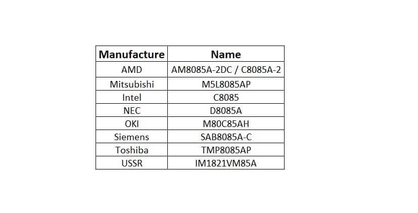
Some second source manufactures also produced CMOS version of the microprocessor 8085 – 80C85. The 8085 was produced at speeds ranging from 3 MHz to 6 MHz.
Introduction to Microcomputer System
The microcomputer system is the interconnection of CPU, memory and input/output devices through the buses.
CPU – Central processing unit is the brain of the microcomputer system. The CPU coordinates the entire microcomputer operation.
Its function is to accept inputs from the input devices depending on the instructions given in the permanent programs stored in the ROM or temporary programs stored in the RAM, execute the programs and finally display the result though the output devices. The CPU chip of a microcomputer is known as the microprocessor.
Memory – Read only memory (ROM) is used for permanently storing the programs and random access memory (RAM) is used for temporary storage.
Peripheral Devices – The input devices and output devices are called as peripheral devices. The input devices are used to feed the data into the microcomputer. The output devices are used to display the result.
- Address Bus
- Data Bus
- Control Bus
The address bus carries the address of a memory location or I/O device that the CPU wants to access. The data bus is used to transfer data between the CPU, memory and I/O devices . The control bus is used to carry necessary control signals between the CPU, memory and I/O devices.

Introduction to Microprocessor
The CPU built on a single IC is called microprocessor. The internal architecture of the microprocessor determines how and what operations can be performed with the data.
To perform any operation, the microprocessor requires registers, an arithmetic logic unit ALU, control logic, instruction register, program counter and internal buses. The block diagram of a microprocessor.
The ALU is the computational unit of the microprocessor which performs arithmetic and logical operations on binary data.
The register array is the internal storage device. The input/output data and any other binary information needed for processing are stored in the register array.
The control unit is generating the necessary control signals for internal and external operations of the microprocessor.
When an instruction is fetched from memory, it is located in the instruction register. The instruction decoder decodes the contents of the instruction register.
Program counter is used to hold the memory address of the next instruction to be executed.
Advantages of Microprocessor
- Low cost
- Small size
- Low power consumption
- High versatility
- High reliability
Microprocessor 8085
Features of 8085
-
- 8085 A is an 8-bit general purpose microprocessor.
- It is a 40 pin dual in line package single chip integrated circuit.
- Only one +5 V power supply is needed for its operation.
- It can operate with a 3 MHz single phase clock.
- The width of the data bus is 8-bit. The width of the address bus is 16-bit. Therefore maximum of 64 kilobytes of memory locations (216 = 65,536 = 64 KB) can be addressed directly by the 8085.
- The multiplexing of address/data bus allows extra control signals.
- 8085 has one non-maskable (TRAP) and three maskable-vectored interrupts.
- It provides serial input data (SID) and serial output data (SOD) lines for simple serial interface.
- 8085 has an inbuilt clock oscillator circuit and requires externally only a crystal. The frequency of the crystal is internally divided by 2. One 8-bit accumulator
Temporary register
Architecture Of Microprocessor 8085
- Accumulator
- General Purpose Registers
- Program Counter (PC)
- Stack Pointer (SP)
- Arithmetic and Logic Unit (ALU)
- Temporary Register
- Flags
- Instruction Register and Decoder
- Timing and Control unit
- Interrupt control
- Serial I/O control
- Address buffer and Address Data buffer
- Address Bus and Data Bus

General Purpose Registers
The 8085 evolution of microprocessor contains six 8-bit general purpose registers. They are B,C,D,E,H and L register. To hold 16-bit data, a combination of two 8-bit register can be employed. The combination of two 8-bit register is known as register pair.
The valid register pairs in the 8085 are B-C, D-E and H-L, The H-L pair is used to act as memory pointer and for this purpose it holds the 16-bit address of memory location. The general purpose registers are accessible to programmer.
Program Counter (PC)
It is a 16-bit special purpose register. It is used to hold the memory address of the next instruction to be executed. It keeps the track of memory addresses of the instruction in a program while they are being executed.
The microprocessor increments the content of the program counter during the execution of an instruction so that it points to the address of the next instruction in the program at the end of the execution of instruction.
Stack Pointer (SP)
Stack pointer is a 16-bit register used as a memory pointer. It maintains the address of the last byte entered into the stack (stack is a portion of RAM). The stack pointer is decremented each time when data is loaded into the stack and is incremented when data is retrieved from the stack.
Arithmetic and Logic Unit (ALU)
The ALU carries out the arithmetic and logic operations 8-bit data. The contents of the accumulator and the temporary register are the input to the ALU.
It can perform arithmetic operations such as addition, subtraction and logical operations such as AND, OR and EX-OR. The ALU result is then stored back in the accumulator.
Temporary Register
It is an 8-bit register associated with ALU. It hold data during an arithmetic/logical operation. It is used by the microprocessor.
Flags
- Carry Flag
- Parity Flag
- Auxiliary Carry Flag
- Zero Flag
- Sign Flag
| Read More Topics |
| Database and database users |
| 8086 Microprocessor intel software aspect |
| Interfacing microcontroller 8225 |